Examples
This page features example processes performed at the Nanoscale Research Facility. Each example has a general process flow with links to the equipment utilized. Click on a title below to scroll to the example details.
AlGaN/GaN High Electron Mobility Transistor (HEMT)
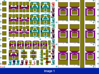
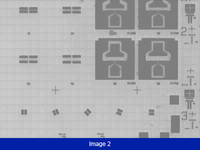
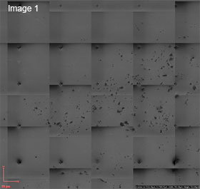
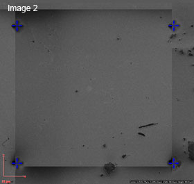
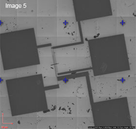
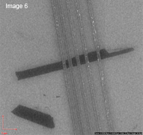
The field of III-N semiconductors has gained a lot of attention for use in high speed and high power switching as well as solid-state sensors. The high electron mobility transistor (HEMT) device layout (image 1) pictured above was fabricated to specification provide by UF researchers. This die layout contains conventional HEMTs with micron and submicron gates fabricated to 250nm gate length. The mask set allowed for three different gate metals to be used on the same die for both materials and process comparisons. A die in process is seen in image 2.
General Process Flow
- Design Layout (created using GDSii editor or Autocad)
- Mask Fabrication
- Photolithography
- Plasma Etch
- Etch Inspection
- Photolithography (refer to step 3)
- Metal deposition
- Anneal
- Photolithography (refer to step 3)
- Metal deposition (refer to step 7)
- Electron Beam Lithography
- Metal deposition (refer to step 7)
- Dicing
- Die Packaging (manual pick and place and die bonding)
- Wire Bonding
Nano-CT & 3D Printer
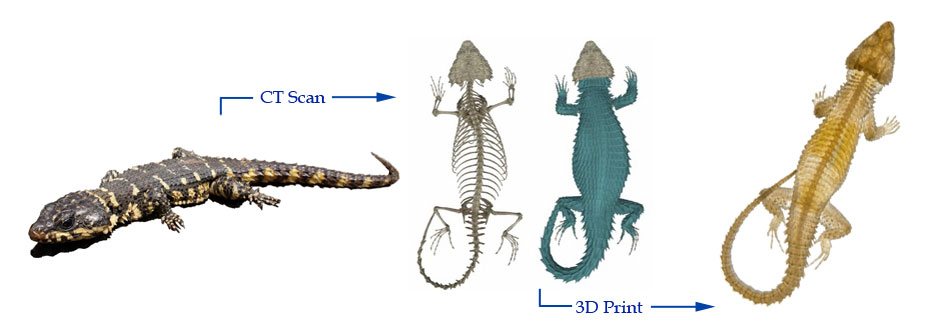
Specimens were scanned with a GE V|tome|xm 240 CT Scanner to obtain high resolution 3D images of the entire specimen. These 3D images were then converted into 3D printer images called stereolithography (SLT) files and printed with different polymers on an Objet260 Connex2 3D printer. For some specimens, the SLT file was enlarged so micron scale details within the specimen could become visible to the naked eye in the 3D printed model.
General Process Flow
- Specimen Scanning
- Scan Processing/Editing
- 3D Printing
Solid-State Sensors
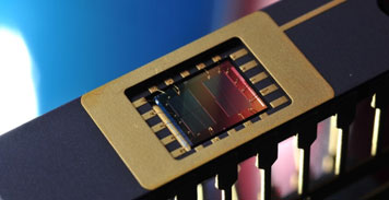
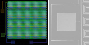
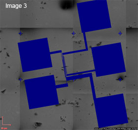
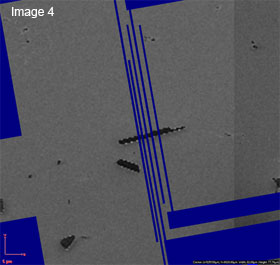
Solid-state sensors are advancing rapidly and are being placed in a wide array of applications from mechanical movement (accelerometers), sounds (microphones), and bio detection (glucose, pathogen). The device pictured above was fabricated to detect radiation doses and map the dose over an area, it consisted of a dense array of 1000 p-i-n diodes.
General Process Flow
- Design Layout
- Mask Fabrication
- Photolithography
- Etch Si Wafer
- Implant Dopants (performed by external vendor)
- Anneal
- Metal deposition
- Metal liftoff, inspection
- Etch Al Metal
- Die Separation
- Die Attach to Package (manual process)
- Wire Bonding
Spiral Mirror Lens on Flat and Curved Surfaces
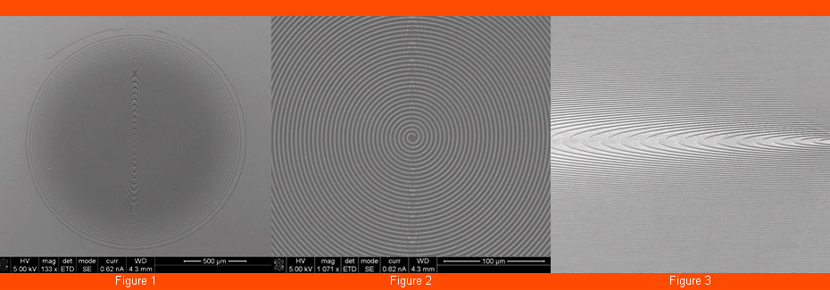 Figure 1: Image of spiral mirror with 500 micrometer scale, Figure 2: Image of spiral mirror with 100 micrometer scale, Figure 3: Image of spiral mirror at an oblique angle -no scale
A spiral designed lens was fabricated on both flat and curved surfaces. The design had a spiral spacing that was graded (with a minimum spacing of 1 micron at the center and 10s of microns at the outer edge) and employed thin gold metal to block a particular wavelength regime. The diameter of the lens spiral was 2mm. The design was created via computer aided design (CAD) software and transferred to an electron beam lithography system to create the pattern in a photoresist. The sample later then underwent metallization via regular lift off processing.
General Process Flow
- Design Layout
- Electron Beam Lithography
- Metal Deposition
- Metal Liftoff, Inspection